PCB CIRCUIT
Product Details:
PCB CIRCUIT Price And Quantity
- 6000.00 - 7000.00 INR/Piece
- 1500 INR/Piece
- 5 Piece
PCB CIRCUIT Trade Information
- Paypal Cash in Advance (CID) Cheque
- 1000 Piece Per Day
- 7 Days
- Yes
- Within a certain price range free samples are available
- Asia Australia Central America North America South America Eastern Europe Western Europe Middle East Africa
- All India Punjab Daman and Diu Uttarakhand Chandigarh Haryana Sikkim Odisha Madhya Pradesh Tripura Pondicherry West Bengal Tamil Nadu Arunachal Pradesh Himachal Pradesh Gujarat Manipur Bihar Meghalaya Mizoram Assam Maharashtra South India Rajasthan Nagaland West India East India Lakshadweep Uttar Pradesh Delhi North India Goa Dadra and Nagar Haveli Jharkhand Jammu and Kashmir Karnataka Andaman and Nicobar Islands Kerala Central India Chhattisgarh Andhra Pradesh Telangana
Product Description
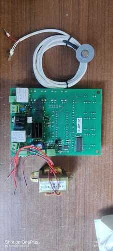
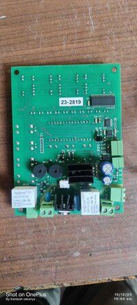
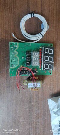
A PCB Printed Circuit Board is a critical component in electronic devices providing both physical support and electrical connections for components Heres a typical content breakdown for a PCB circuit product
1 PCB Material
Substrate The base material typically FR4 a type of fiberglass provides structural support
Copper Layers Copper is used to form conductive traces pads and vias that connect different components
Soldermask A protective layer that prevents accidental shorts and protects copper traces
Silkscreen Printed markings that provide information like component labels logos and orientation
2 Components
Active Components
Resistors Limit the flow of current
Capacitors Store and release electrical energy
Transistors Act as switches or amplifiers
Diodes Allow current to flow in one direction only
Integrated Circuits ICs Multifunctional devices such as microcontrollers logic gates amplifiers etc
Passive Components
Inductors Store energy in a magnetic field
Oscillators Produce regular electrical signals
3 Connectors
Pin headers Used to attach external devices or other PCBs
SMD Surface Mount Device connectors For highdensity interconnects
4 Vias
ThroughHole Vias Holes that go through the board to connect different layers of the PCB
BlindBuried Vias Vias that connect specific layers without going all the way through
5 Power Management
Power Rails Provide different voltage levels eg 5V 12V
Voltage Regulators Ensure that components receive the correct voltage
Protection Circuits Prevent overvoltage overcurrent and electrostatic discharge ESD
6 Traces and Routing
Signal Traces The copper paths that connect various components
Ground Plane A large continuous copper layer that helps with noise reduction and provides a common reference point for all components
Power Plane A dedicated layer for power distribution across the PCB
7 Soldering and Assembly
Soldering Process Components are either soldered throughhole or mounted as SMD SurfaceMounted Devices
Automated Soldering Machines For mass production
Hand Soldering Used for prototyping or final adjustments
8 Testing and Quality Control
Visual Inspection Checking for soldering defects or incorrect component placement
Electrical Testing Ensures all connections are working and the circuit behaves as expected
Thermal Cycling Ensures the PCB can withstand extreme temperature conditions
9 Protection and Coating
Conformal Coating Protects the PCB from moisture dust and other contaminants
Epoxy Coating Used in some designs for added protection or insulation
10 Mechanical Design
Outline and Dimensions The physical shape of the PCB including mounting holes
Cooling Systems Heat sinks or thermal vias to dissipate heat from highpower components
This comprehensive structure forms the backbone of any PCBbased electronic product ensuring it functions properly remains durable and integrates well with other parts of the system A PCB Printed Circuit Board is a critical component in electronic devices providing both physical support and electrical connections for components Heres a typical content breakdown for a PCB circuit product
1 PCB Material
Substrate The base material typically FR4 a type of fiberglass provides structural support
Copper Layers Copper is used to form conductive traces pads and vias that connect different components
Soldermask A protective layer that prevents accidental shorts and protects copper traces
Silkscreen Printed markings that provide information like component labels logos and orientation
2 Components
Active Components
Resistors Limit the flow of current
Capacitors Store and release electrical energy
Transistors Act as switches or amplifiers
Diodes Allow current to flow in one direction only
Integrated Circuits ICs Multifunctional devices such as microcontrollers logic gates amplifiers etc
Passive Components
Inductors Store energy in a magnetic field
Oscillators Produce regular electrical signals
3 Connectors
Pin headers Used to attach external devices or other PCBs
SMD Surface Mount Device connectors For highdensity interconnects
4 Vias
ThroughHole Vias Holes that go through the board to connect different layers of the PCB
BlindBuried Vias Vias that connect specific layers without going all the way through
5 Power Management
Power Rails Provide different voltage levels eg 5V 12V
Voltage Regulators Ensure that components receive the correct voltage
Protection Circuits Prevent overvoltage overcurrent and electrostatic discharge ESD
6 Traces and Routing
Signal Traces The copper paths that connect various components
Ground Plane A large continuous copper layer that helps with noise reduction and provides a common reference point for all components
Power Plane A dedicated layer for power distribution across the PCB
7 Soldering and Assembly
Soldering Process Components are either soldered throughhole or mounted as SMD SurfaceMounted Devices
Automated Soldering Machines For mass production
Hand Soldering Used for prototyping or final adjustments
8 Testing and Quality Control
Visual Inspection Checking for soldering defects or incorrect component placement
Electrical Testing Ensures all connections are working and the circuit behaves as expected
Thermal Cycling Ensures the PCB can withstand extreme temperature conditions
9 Protection and Coating
Conformal Coating Protects the PCB from moisture dust and other contaminants
Epoxy Coating Used in some designs for added protection or insulation
10 Mechanical Design
Outline and Dimensions The physical shape of the PCB including mounting holes
Cooling Systems Heat sinks or thermal vias to dissipate heat from highpower components
This comprehensive structure forms the backbone of any PCBbased electronic product ensuring it functions properly remains durable and integrates well with other parts of the system

Price:
- 50
- 100
- 200
- 250
- 500
- 1000+
Other Products in 'Warmer' category
 |
KORRIDA MEDICAL SYSTEMS
All Rights Reserved.(Terms of Use) Developed and Managed by Infocom Network Private Limited. |

 Send Inquiry


